 |
|||
|
|
|||
|
Page Title:
Figure 5-34. TD Card, Pulse Transition Code - Waveform Diagram |
|
||
| ||||||||||
|
|
 T.O. 31W2-2GSC24-2
TM 11-5805-688-14-1
NAVELEX 0967-LP-545-3011
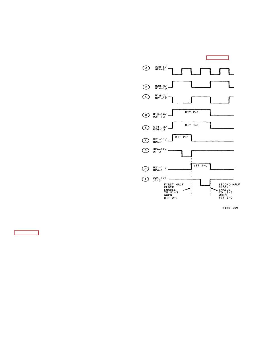
Read address counter U2 is incremented by the read
half transition, AND gate U24- 12 generates a positive-
clock pulses from inverter U19-6 in the APLL circuit. The
going clock pulse to data buffer U1-5 in the second half
data pulses from the elastic storage register are serially
cycle of the timing as shown in (I) of figure 5-34.
clocked through AND gates U9-8 and U9-11 and OR
gate U9-6 to shift register U14 in the transition decoder
No. 1 circuits.
5-437. The transition decoder No. 1 circuits decode
each set of 3-bit transition codes into the original data
transition that occurred in the far-end multiplexer. The
overall result is that data output buffer U1-5 generates
re- constructed data pulses that are identical to those
originally applied to the far-end multiplexer. The 3-bit
code is loaded serially into 3-bit shift register U14 and is
clocked out as a 3-bit parallel output. Bit 1 read out of
Q2 of U14 is the transition code and is always a one
each time a transition occurs. This bit is applied through
AND gate U20-11 and inverter U19-10 as an enable
input to pin 13 of AND gate U24- 12. Bit 2, which
identifies when the transition occurred, is a one when
the transition occurred in the first half of the timing pulse
or bit 2 is a zero when the transition occurred in the
second half of the timing pulse. The bit 2 (Q1) output
from U14 is applied to one input of exclusive OR gate
U21- 11. The bit 3 (QO) output from U14 indicates that
the transition is a positive-going (one) signal or a
negative- going (zero) signal. The QO output is applied
directly to the D input of data output buffer U1-5.
5-438. The second input to exclusive OR gate U21-11 is
a timing signal from U18-7 in the APLL circuit. This
clock signal is applied at the same clock rate as the
clock signal applied to U14-10. The clock signal applied
to pin 2 of AND gate U24-12 is twice the frequency of the
clock signal applied to U14-10. When bit 2 is a one,
Figure 5-34. TD Card, Pulse Transition Code -
indicating a first half transition, AND gate U24-12
Waveform Diagram
generates a positive-going clock pulse to data buffer U1-
5 in the first half cycle of the timing as shown in (G) of
5-116
|
|
Privacy Statement - Press Release - Copyright Information. - Contact Us |
