 |
|||
|
|
|||
|
Page Title:
Figure 5-33. TD Card, 3-Bit Transition Code - Waveform Diagram |
|
||
| ||||||||||
|
|
 T.O. 31W2-2GSC24-2
TM 11-5805-688-14-1
NAVELEX 0967-LP-545-3011
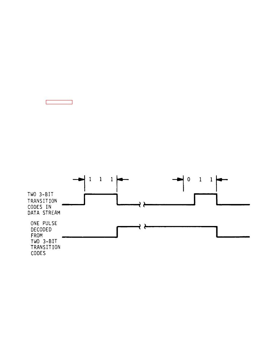
The read address counter that produces the 4-bit read
address counter and the clock signals to the transition
addresses to the data elastic storage is incremented by
decoder are produced by the APLL circuit. The read
the read clock signals from the analog phase-locked loop
clock signals to the read ad- dress counter are phase
(APLL) circuit. The data read out of the data elastic
locked to the write clock signals by the APLL circuit to
storage register are clocked into the transition decoder
ensure that the number of read clocks applied to the
No. 1 circuits. In the transition decoder No. 1 circuits,
read address counter equals the number of write clock
each set of 3-bit transition codes is decoded to produce
(DGCXX) signals applied to the write address counter.
one positive-going or negative-going transition enable
The smoothing function per- formed by the APLL circuit
signal that clocks the data out- put buffer. The data from
described in the SB card theory of operation is also
data output buffer No. 1 are routed to the data output
performed by the APLL circuit on the TD card. The
drivers circuit. Figure 5-33 shows a typical pulse output
overall operation of the APLL circuit is the same as that
produced from the data output buffer as a result of
described for the SB card. Basically, the phase detector
decoding two sets of 3-bit transition codes. The data
monitors the count eight out- puts from the read and
applied to the data output drivers circuit are conditioned
write address counters and generates corrective signals
and then applied through the data output line switch
to the active filter circuit when a phase change is
circuit to pro- duce a balanced or unbalanced output
detected between the negative-going transitions of the
from the TD card.
In a balanced line output
write and read address pulses. In turn, the active filter
configuration, two complementary channel data out
circuit generates the sloping dc control voltage that
signals (DOXX and DOXX-) are produced. Only one
controls the voltage-controlled multivibrator (VCM) output
output signal (DOXX) is produced in the unbalanced line
frequency. The output from the VCM is applied to the
output configuration.
divide-by-2n counter. The counter, in turn, generates
the read clock pulses applied to the read address
counter in the input-output buffer function.
5-430. APLL Circuit. The read clock signals to the read
6186-158
Figure 5-33. TD Card, 3-Bit Transition Code - Waveform Diagram
5-114
|
|
Privacy Statement - Press Release - Copyright Information. - Contact Us |
