 |
|||
|
|
|||
|
Page Title:
Figure 5-23. GC/DM Card, Gated Clock Generation Circuits - Block Diagram |
|
||
| ||||||||||
|
|
 T.O. 31W2-2GSC24-2
TM 11-5805-688-14-1
NAVELEX 0967-LP-545-3010
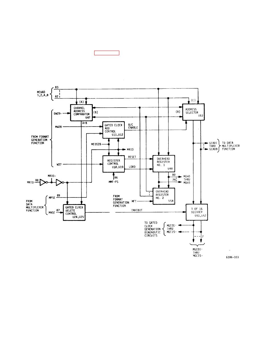
GC/DM card. During each data word, one gated clock
Minor frame count MMFC1 is applied to the minor frame
signal is generated for each used (active or strapped)
activity detector circuit in the diagnostic function.
port in the multiplexer configuration. The total number of
gated clocks generated during one word period is a
5-315. Gated Clock Generation Function (Figure 5-23)
preset variable between 15 and 31. Each used port in a
multiplexer configuration is assigned to one of the active
5-316. Gated clock signals are generated and applied
channels. The gated clock signal generated for a given
to the RCB and TE/TR channel cards to systematically
used port carries the channel address of the active
clock channel data out of storage registers on the
channel to which it is assigned. For example, if active
channel cards to the output data multiplexer on the
channel No. 1 has four used ports, it will
Figure 5-23. GC/DM Card, Gated Clock Generation Circuits - Block Diagram
5-81
|
|
Privacy Statement - Press Release - Copyright Information. - Contact Us |
