 |
|||
|
|
|||
|
Page Title:
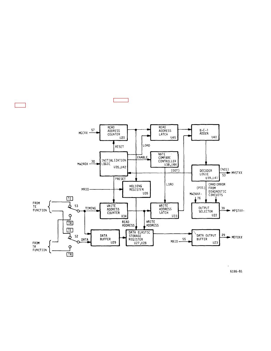
Figure 5-18. TE/TR Card, Rate Conversion Buffer Circuits - Block Diagram |
|
||
| ||||||||||
|
|
 T.O. 31W2-2GSC24-2
TM 11-5805-688-14-1
NAVELEX 0967-LP-545-3010
5-216. The incoming data pulses (DIXX) are
5-218. The RCB functional circuits are basically the
conditioned in the data receiver and are then applied to
same as those described for the RCB card. The data
the transition detector and to the RCB function. The
pulses from the TE or TR circuits are clocked through
transition detector, in turn, generates a reset signal to the
the appropriate TE or TR position of switch S3 by the
two counters each time a positive-going or negative-
associated TE or TR timing pulses. The data pulses are
going pulse transition is detected. Since the output of the
applied through the data buffer to the data elastic
counters is the same frequency as the incoming data,
storage register.
the MSB from the divide-by-32 counter should occur as a
synchronized center sample pulse to clock the
5-219. The data elastic storage register is a 16-port
conditioned data pulse applied to the RCB function from
register that has the capability for data bits to be written
the data receiver.
into the register at the same time that stored data are
read out (at a different address). The write address
5-217. Rate Conversion Buffer (RCB) Function (Figure
counter,
which
is
sequentially
incremented
Figure 5-18. TE/TR Card, Rate Conversion Buffer Circuits - Block Diagram
5-55
|
|
Privacy Statement - Press Release - Copyright Information. - Contact Us |
