 |
|||
|
|
|||
|
Page Title:
Figure 5-17. TE/TR Card, Timing Recovery Circuits - Block Diagram |
|
||
| ||||||||||
|
|
 T.O. 31W2-2GSC24-2
TM 11-5805-688-14-1
NAVELEX 0967-LP-545-3010
6186-80
Figure 5-17. TE/TR Card, Timing Recovery Circuits - Block Diagram
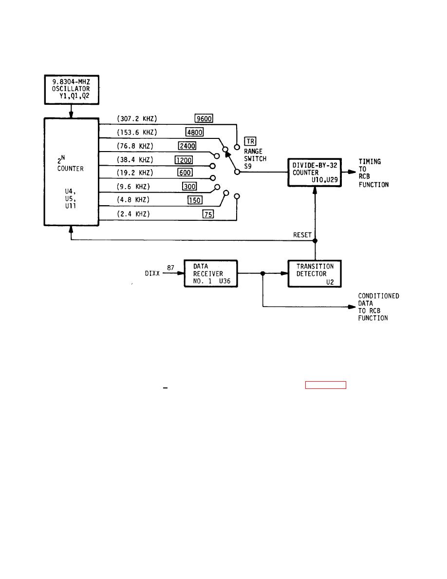
applied data bit rate variation being within +250 ppm and
counter as shown in figure 5-17. The eight outputs are
the isochronous distortion of the data pulses being less
developed by the counter performing a binary count
than 40 percent. A decrease in data rate variation and/or
down of the output from the 9.8304-MHz oscillator. The
N
binary outputs from the 2 counter are actually 32 times
isochronous distortion results in a corresponding
the bit rate selected. For example, the output from the
increase in bit count integrity.
counter that is applied to the divide-by-32 counter from
the 300 position of the TE range switch is 9600 Hz (32 x
5-215. Initially, the TR range switch is set to the switch
300). Therefore, the timing bit rate applied to the RCB
position that is equal to the incoming data bit rate. The
function from the counter is the actual frequency
N
switch selects one of the eight outputs from the 2
selected by the TE range switch.
5-54
|
|
Privacy Statement - Press Release - Copyright Information. - Contact Us |
