 |
|||
|
|
|||
|
Page Title:
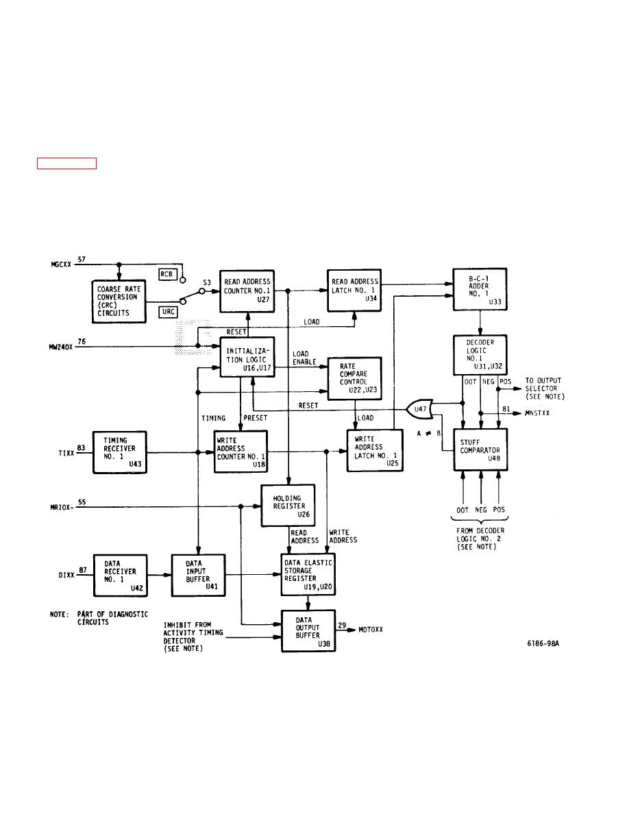
Figure 5-12. RCB Card-Block Diagram |
|
||
| ||||||||||
|
|
 T.O. 31W2-2GSC24-2
TM 11-5805-688-14-1
NAVELEX 0967-LP-545-3011
receiver No. 1 are applied to the data input buffer
circuits (fine rate adjustment) will cause the addition or
circuit. The incoming channel timing pulses (TIXX) are
deletion of gated clocks not controlled through the
also converted to TTL levels. The conditioned timing
coarse rate conversion circuits.
pulses from timing receiver No. 1 are applied to the
data input buffer, rate compare control, write address
5-174. Detailed Functional Block diagram Discussion
counter, initialization logic, and the diagnostic function.
5-176. The conditioned data pulses are clocked by the
5-175. Input-Output Data Buffer Function.
The
associated timing pulses through the data buffer and
incoming channel data bits (DIXX) are applied to data
are applied serially to an elastic storage register. The
receiver No. 1, where the data pulses are converted to
elastic storage register is a
TTL levels. The conditioned data pulses from data
Figure 5-12. RCB Card-Block Diagram
Change 1 5-41
|
|
Privacy Statement - Press Release - Copyright Information. - Contact Us |
