 |
|||
|
|
|||
|
Page Title:
Figure 2-10. Typical transistor AND gate circuit. |
|
||
| ||||||||||
|
|
 TM 11-6625-667-45/NAVSHlPS 0969-249-8010/NAVAIR 16-30APM123-2TO 33A1-3-367-22
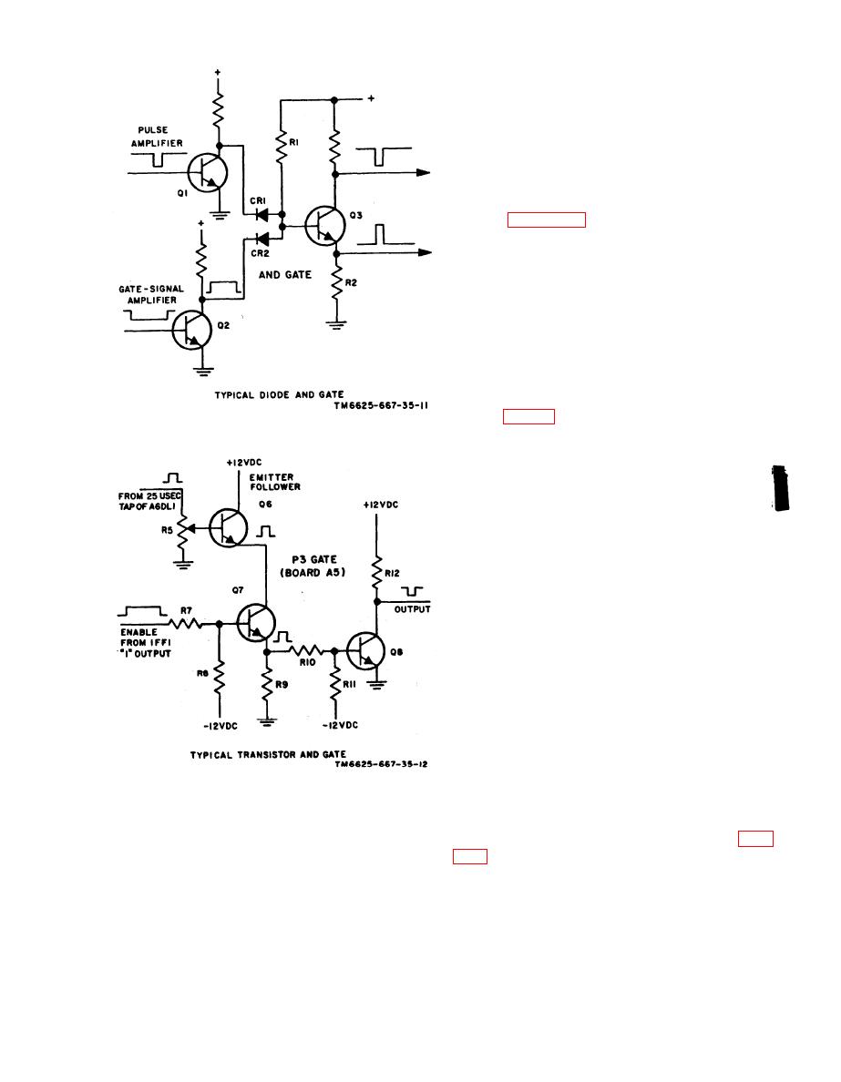
am gated, Q3 conducts. Two outputs are shown at
Q3. If the gate is used as an inverter, the collector
out put. is used and the output developed across
emitter resistor R2 is not used. This type of gate is
known as a NAND (negative AND) gate because
it performs an inverting function. If the gate is
not. used for inversion, the circuit used is an
emitter follower and the output is taken across
R2. This gate is known as an AND gate.
(2) Figure 2-10 illustrates a typical transis-
tor AND gate. Gate inputs are applied to the col-
lector and base of gate transistor Q7. In this
circuit, emitter follower Q6, when conducting,
-effectively connects the collector of Q7 to the +12-
volt dc source. When an enable voltage is applied
to the base of Q7, a positive pulse arriving from
Q6 will cause conduction. The emitter output of
Q7 causes gate transistor Q8 to conduct, and the
gated pulse is taken from its collector.
2-11. Encoder Basic Logic Analysis
Figure 2-9. Typical diode AND gate circuit.
a. Encoder Enabling and Line-Drive Genera-
tion. When PRESS-TO-TEST switch A15S4
pressed, the prf generator generates 2.17 milli-
second pulses at a 230-pps rate. This pulse rate is
adjusted by means of control A5R31. The trailing
edge of each pulse is used to trigger line-drive
generator ISS1 and to set encode enable IFF1.
(1) Line-drive generator ISS1 is a single-
shot and contains transistors A4Q1 and A4Q2.
Transistor A4Q1 is normally not conducting and
provides the "0" output, and A4Q2 is normally
conducting and provides the "1" output. When
triggered by the prf generator, the "0" output goes
low and the "1" output goes high. This produces
0.7-microsecond, negative-going pulses at the "0"
output and positive-going pulses at the "1" output.
The positive-going outlet is used for mode 4 pre-
triggers during mode 4 tests. The negative-going
(0) output is gated and inverted, then coupled by
delay line driver A10Q7 to delay line A6DL1. The
pulse width of ISS1 is adjusted by A4R6.
Figure 2-10. Typical transistor AND gate circuit.
(2) Encode enable IFF1 provides enabling
voltages to the delay line output AND gates (P1
when the positive output. of Q1 blocks gate diode
and P3) and enables receiver video gate 2 (para
CR1. The gate diodes control the conduction of
transistor Q3 and when the pulses from Q1 and Q2
2-15
Change 4
|
|
Privacy Statement - Press Release - Copyright Information. - Contact Us |
