 |
|||
|
|
|||
|
Page Title:
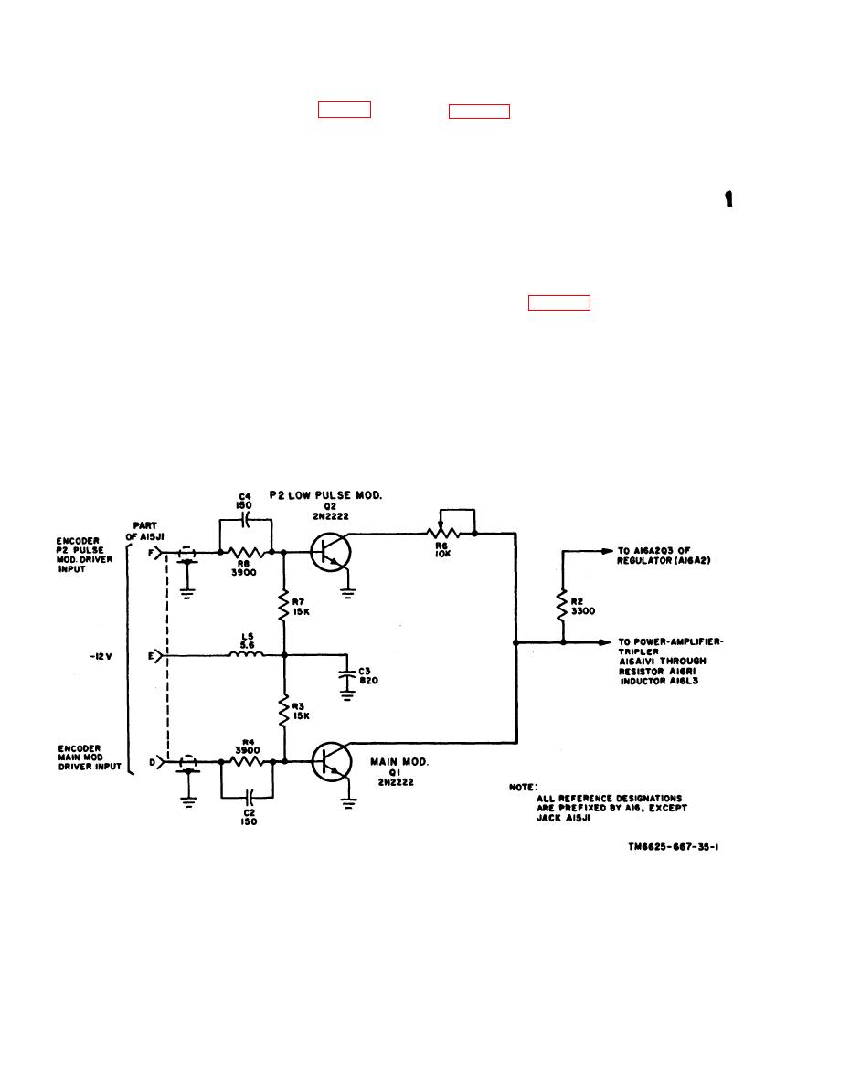
Figure 2-11. Low P2 pulse and main modulator, simplified diagram. |
|
||
| ||||||||||
|
|
 TM 11-6625-667-45/NAVS141PS 0969-249-8010/NAVAIR 16-30APM123-2/TO 33A1-3-367-22
C2 is used to adjust the RF coupling to PROBE
2-13. Receiver Section, Preselector A15Z1
jack A15J24.
and Detector A15Z2
maintains a constant dc voltage at the cathode of
a. Preselector A16ZI. Preselector A15Z1 is a
A16A1V1 and electron tube filaments. The regu-
passive resonant cavity. It is adjusted to 1,090 mc
lator output is preadjusted with control A16A2R1
0.5 and provides receiver selectivity of 6.5 mc 1
to + 18.5 0.5 volts at test point A16TP4. This.
at the 3-db points of the selectivity curve. The RF
voltage is critical since transmitter power level
reply received at PROBE jack A15J24 is passed
and electron tube life are affected by departures
through preselector A15Z1 and coupled to detector
from this level. Transistor A16A2Q1 senses regu-
A15Z2. Crystal diode CR1 of A15Z2 demodulates
lator output changes through Capacitor A16A2C1.
the RF and applies the demodulated signal to the
An output voltage increase causes increased con-
video amplifier input stage (b below).
duction, and a voltage decrease causes decreased
conduction. The transistor collector output goes
fiers Q1 and Q3 (fig. 2-12) provide receiver
low or high, respectively, and controls the conduc-
sensitivity-control and amplifies the reply video.
tion of emitter followers A16A2Q2 and A16A2Q3;
The gain of video amplifier (Q1 is adjusted by
therefore, these transistor produce corresponding
sensitivity control A8R5 and determines receiver
voltage changes at the regulator output (A16A
sensitivity. Reply video from detector A15Z2
2Q3). This action nullifies input voltage changes.
coupled by capacitor A8C3, causes A8Q1 to con-
duct. The negative output voltage from the col-
Regulator diodes A16A2VR1, A16A2VR2, and
lector of A8Q1 decreases the conduction of A8Q2
A16A2VR3 maintain a constant bias at the
proportionately. The output video level to video
emitter and base of A16A2QL
Figure 2-11. Low P2 pulse and main modulator, simplified diagram.
2-18
Change 4
|
|
Privacy Statement - Press Release - Copyright Information. - Contact Us |
