 |
|||
|
|
|||
|
Page Title:
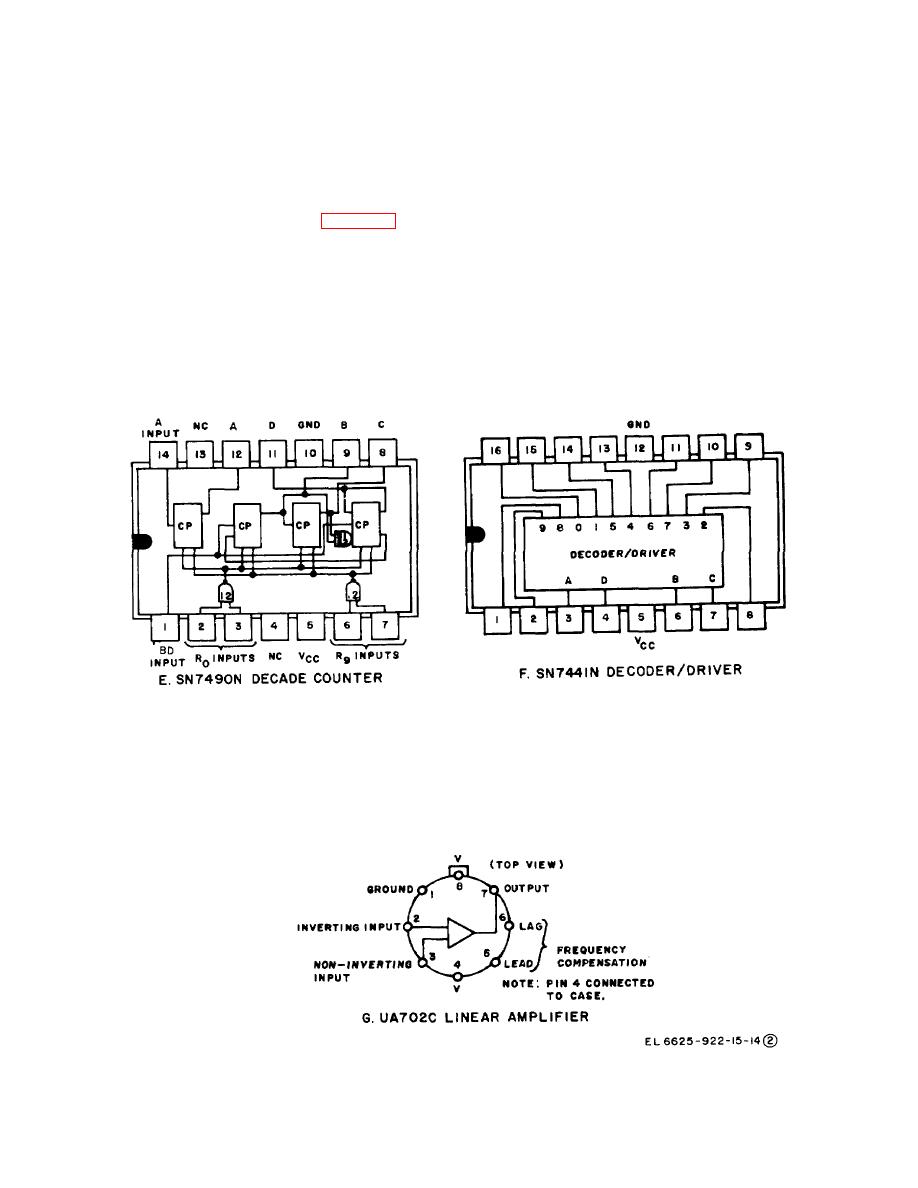
Figure 5-6(2). Pin connections of integrated circuits (part 2 of 2). |
|
||
| ||||||||||
|
|
 TM 11-6625-922-15
Transistors Q4 and Q7 together give a voltage gain of
follower Q17. The vfo signal and the modulated 2-MHZ
signal are mixed in stage Q13, 14; the output is sent to
slightly less than unity, with feedback from the emitter to
the base of Q4. Four active filter sections in cascade
compound emitter-follower Q15, Q16, and then to a low-
provide the desired frequency response; near unity gain
pass inductance-capacitance (lc) network to select only
from dc to near 25Hz, then rapid attenuation of higher
the difference frequency, 0- to 600-kHz modulated sine
frequency components. An external variable resistor
wave.
(front panel DELAY ZERO ADJ control) is used across
R16 in the fourth stage to give a variable phase shift for
operation of this circuit is similar to that of the 2-MHz
setting initial conditions. The input at pin V is a signal
modulator mixer. The inputs are a 200 kHz square
with 25 Hz modulation; the output at pin Y is the 25-Hz
wave, a sine-wave modulating signal at pin A, and a vfo
sine wave. The operation of the 83-1/3-Hz and 250-Hz
200- to 260-khz square wave.
The output is a
active filters are similar. Resistors R61, R63, and R65
modulated sine wave, between 0 and 60 khz.
are selected values used only on A13 to give a fixed
f. Low-Pass Active Filters 1A7 and A13 (fig. 9-
phase shift in the filters. On A7, the phase shift is
13). Transistors Q4 and Q7 represent a single active
adjustable by the DELAY ZERO ADJ front panel control.
filter section. The products of R13 and C4, and R16 and
C7 determine the cutoff frequency of the low-pass filter.
Figure 5-6(2). Pin connections of integrated circuits (part 2 of 2).
5-11
|
|
Privacy Statement - Press Release - Copyright Information. - Contact Us |