 |
|||
|
|
|||
|
Page Title:
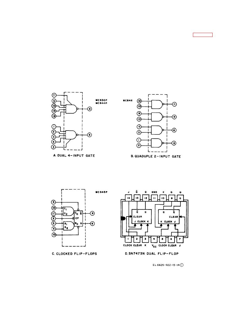
Figure 5-6(1). Pin connections of integrated circuits (part 1 of 2). |
|
||
| ||||||||||
|
|
 TM 11-6625-922-15
produced at the sweep sync output at the start of each
Resistors R25 and R27 shift the dc level of the output
sweep.
signal so that the baseline at pin E is about -3 volts,
instead of 0 volt at pin C. Resistors R32, R33, and R52
are used in a network to generate test voltages to the
circuit has three inputs: 2 MHz square wave, sine-wave
input of the operational amplifier for statically
modulating signal (25, 83-1/3, or 250 Hz), and a vfo 2-
determining the end frequencies when ii the sweep
to 2.6--MHz square wave. The output is a modulated
mode. The resistors are switched in and out by the
sine wave, between 0 and 600 kHz. Transistors Q1 and
SWEEP CALIBRATE switch. Transistor Q14 is a
Q5 are emitter-follower buffers for the 2-MHz and
switching circuit the input at pin R of which is the output
modulating signals, respectively. The two frequencies
of the variable frequency oscillator, 8 to 10.4 MHz.
are mixed ill Q3, then fed to two 2-MHlz tuned amplifier
Integrated circuit M2 operates as a divide-by-4 and M1
stages, Q7, Q8 and Q9, Q10. Transistors Q11 and Q12
is a divide-by-10, giving square-wave outputs between
comprise a compound emitter follower. The vfo input is
ground and approximately +5 volts. A positive pulse is
sent to amplifier Q18 and emitter
Figure 5-6(1). Pin connections of integrated circuits (part 1 of 2).
5-10
|
|
Privacy Statement - Press Release - Copyright Information. - Contact Us |