 |
|||
|
|
|||
|
Page Title:
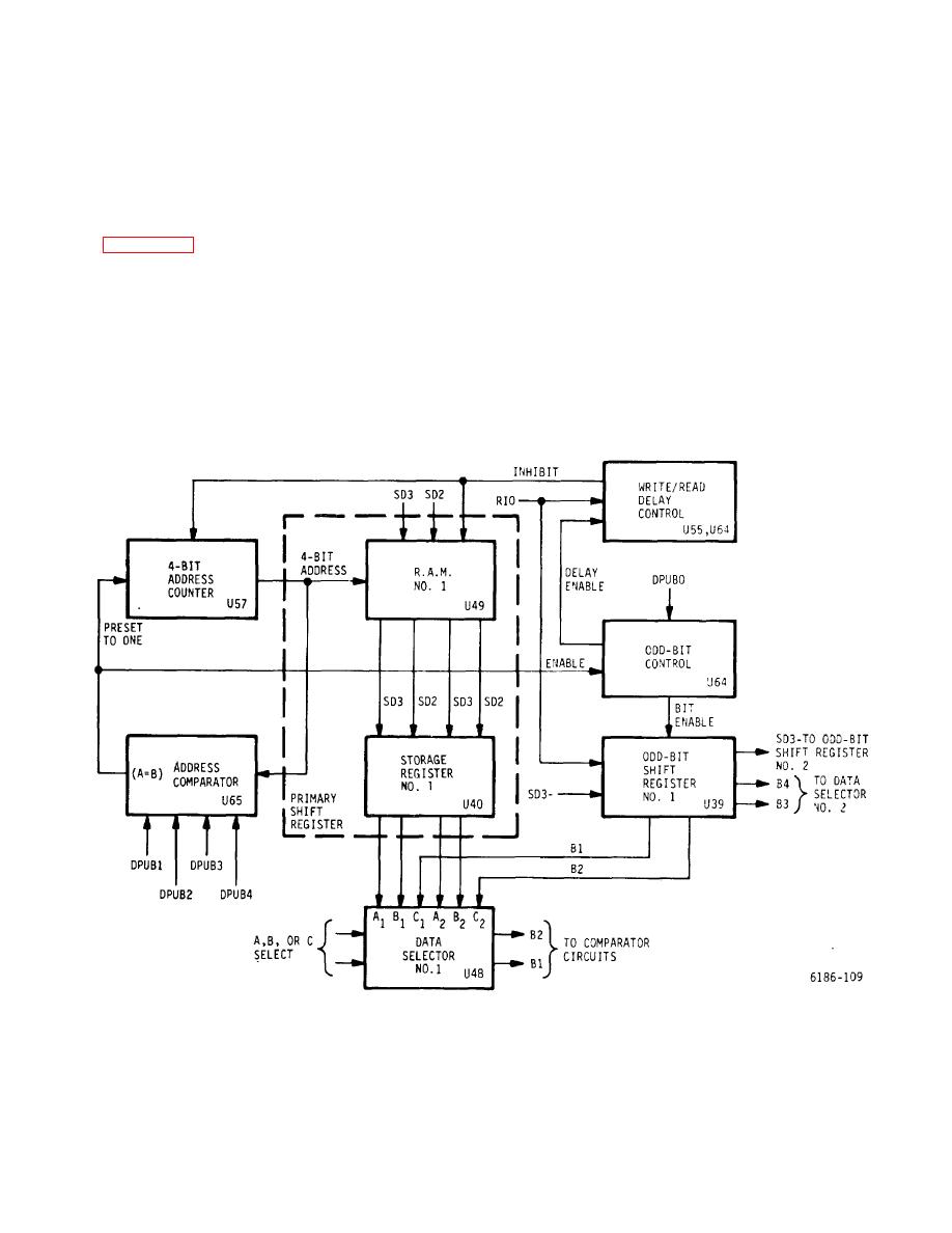
Figure 5-37. FS Card, Primary and Odd Bit Shift Registers - Block Diagram |
|
||
| ||||||||||
|
|
 T.O. 31W2-2GSC24-2
TM 11-5805-688-14-1
NAVELEX 0967-LP-545-3011
The procedure continues through R.A.M. No. 5 to
the address comparator could be part of binary count 31
obtain the de- sired B1 through B10 outputs that form the
or 32. When the 4-bit address counter is preset to a
complete 10-word delay.
count of zero, the truncation occurs after 16 addresses
and access to 32 data bit locations in the R.A.M. have
5-493. Figure 5-37 shows the odd-bit shift register and
been performed. This would be satisfactory for a 32-bit
the primary shift register in an odd-bit application. The
application, but not for the maximum 31-bit application in
operation of the primary shift register in this equipment
this equipment. In turn, presetting the address counter
configuration is the same as described previously, with
to a count of one limits the maximum truncation to occur
one exception. When the address comparator makes a
after 15 addresses and access to 30 data bits to the
compare, the A=B signal presets the primary shift
R.A.M. have been performed. After the A=B condition is
register to a count of one instead of zero. Note that the
obtained in the odd-bit con- figuration, the primary shift
address comparator has only the four MSB's of the
register operation is delayed for one RIO time while one
ports-in-use signals (DPUB1 through DPUB4) applied to
odd data bit is processed as described in the following
select the count that causes the 4-bit address counter to
paragraph.
truncate. Therefore, a binary count of 1111 applied to
Figure 5-37. FS Card, Primary and Odd Bit Shift Registers - Block Diagram
5-129
|
|
Privacy Statement - Press Release - Copyright Information. - Contact Us |