 |
|||
|
|
|||
|
Page Title:
Figure 5-32. SB Card, Coarse Rate Conversion Circuits - Block Diagram |
|
||
| ||||||||||
|
|
 T.O. 31W2-2GSC24-2
TM 11-5805-688-14-1
NAVELEX 0967-LP-545- 3011
After division by a divide-by-2n counter, the output of the
These control signals produce positive-going control
VCM is applied as a clock signal to read address counter
voltages to the VCM.
U21. As shown in figure 5-31, part A, the divided output
frequency of the VCM is gradually decreased over an
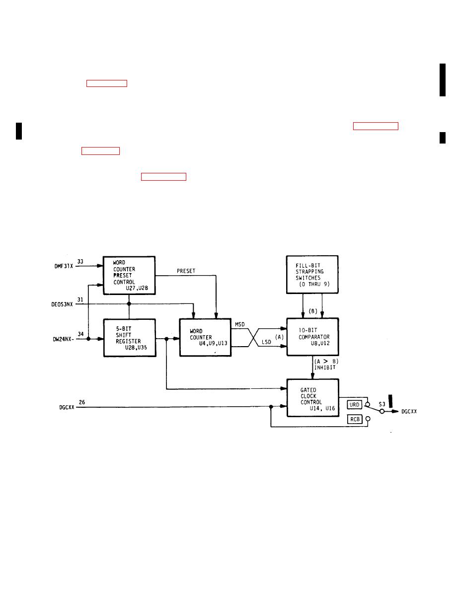
5-404. Coarse Rate Conversion Circuits. The circuits
interval of 1000 or more data bit times. At the end of this
in the coarse rate conversion circuits on the SB card are
period, it is once again nominally equal to the gated clock
identical to those on the RCB card. The functional
rate, as evidenced by the lack of an dc control voltage
application of the two circuits is also identical. The
from phase detector U20. It should be noted that an
coarse rate conversion circuits (figure 5-32) produce
equal number of clocks is applied to write address
modified gated clocks to the write address counter when
counter U18 and to read address counter U21 over the
switch S3 is set to the URD position. In normal
period shown in figure 5-31. This indicates that a long-
operation, end-of-scan signal DEOS3NX increments the
term reduction has been made in the read counter clock
word counter to generate a 10-bit binary code that
rate in response to a short-term rate change in the gated
sequentially advances one count during each word until
clock driving the write counter. Figure 5-31, part B,
the end-of-scan signal in word 24 of minor frame count
illustrates APLL operation in the inverse (positive
31 occurs. At this time, the word counter preset control
stuffing) situation (i.e., long-term increase of the read
generates a preset signal that presets the word counter
clock rate in response to a short-term increase in the
binary output to zero.
gated clock rate). In this case, a series of less positive
control voltages are generated from the phase detector.
Figure 5-32. SB Card, Coarse Rate Conversion Circuits - Block Diagram
Change 1 5-107
|
|
Privacy Statement - Press Release - Copyright Information. - Contact Us |
