 |
|||
|
|
|||
|
|
|||
| ||||||||||
|
|
 T.O. 31W2-2GSC24-2
TM 11-5805-688-14-1
NAVELEX 0967-LP-545-3010
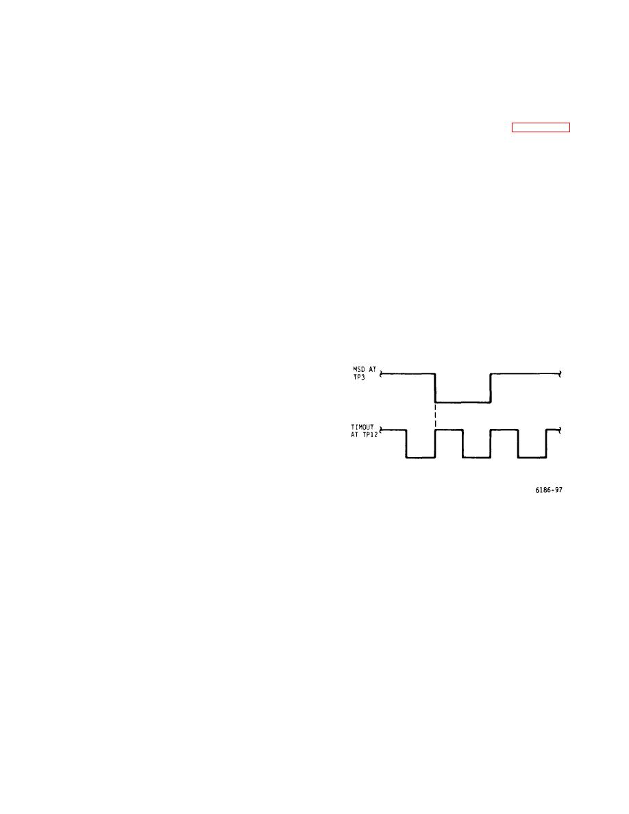
preset. The switch is set so that timing out signals
5-379. DETAILED CIRCUIT DISCUSSION.
TIMOUT and TIMOUT are in phase with the serial digital
data output pulses (MSD) as shown in figure 5-30. The
5-380. Timing Circuits.
timing signals from the phase-adjust circuit are applied
through polarity switch S1 to amplifiers Q1 and Q2 in the
5-381. System clock signal Ro is developed from timing
timing output drivers circuit. Polarity switch S1 is used in
signals TIMIN and TIMIN-, which are applied from an
system configurations to change the polarity of the timing
external source, or Ro is developed from timing oscillator
pulses with respect to the digital data pulses. Transistor
Y1 on the card. Selection of the timing source is made
Q3 is a constant current source for amplifiers Q1 and
by strapping switch S5 to its EXT or INT position. The
Q2. Amplifiers Q1 and Q2 in turn, drive push-pull
oscillator is a plug-in module that provides one base
emitter-followers Q4 through Q7. Setting switch S2 to
frequency selected for a given system application. The
the balanced position (B) connects breakdown diodes
oscillator or the external timing input frequency is
VR2 and VR4 (2.4 vdc) in parallel with breakdown diodes
selectable within the range of 155 Hz to 10 MHz.
VR3 and VR5 (5.6 vdc) in the base circuit of emitter-
However, the 15-stage binary counter permits a source
followers. This balanced configuration produces
signal within the range of 5 MHz to 10 MHz to cover all of
balanced +3-volt TIMOUT and TIMOUT signals. Switch
the desired frequencies within a given system
S2 in the unbalanced position (U) connects only
configuration. When the external source is used, the
breakdown diodes VR3 and VR5 into the base circuit of
TIMIN and TIMIN signals are applied to differential line
the emitter-followers so that a +6-volt TIMOUT signal is
receiver U8. The line receiver processes the incoming
generated and TIMOUT signal output from the card is
digital timing signals into TTL logic levels, which, in turn,
grounded. Diodes CR2 and CR3 in the collector circuits
are applied to switch S5. The signals through S5 are
of Q1 and Q2
applied to the first stage of the 15 stage binary counter,
to switch position S6-1, and to one-shot multivibrator U10
in the loss-of-time activity detector.
5-382. The timing signals through switch S5 are routed
through inverter U3 to J-K flip-flop U1 in the 15-stage
binary counter. The four J-K flip-flops (U1, U4) perform
a high-speed divide-by-16 of the incoming timing signals
to provide outputs to pins 2 through 5 of switch S6.
Four-bit binary counters U6, U7, and U2 perform divide-
by-32 through divide-by-32768 of the incoming timing
signals to provide outputs to pins 6 through 16 on switch
S6. The timing output signal strapped through switch S6
Figure 5-30. RT Card, Reference Timing - Waveform
is system clock signal Ro that is applied to inverter U3 in
Diagram
the phase-adjust circuit. Signal Ro is also routed through
inverters U5, which perform a buffer function, to the OEG
card.
5-383. Switch S3 in the phase-adjust circuit is factory
5-101
|
|
Privacy Statement - Press Release - Copyright Information. - Contact Us |
