 |
|||
|
|
|||
|
Page Title:
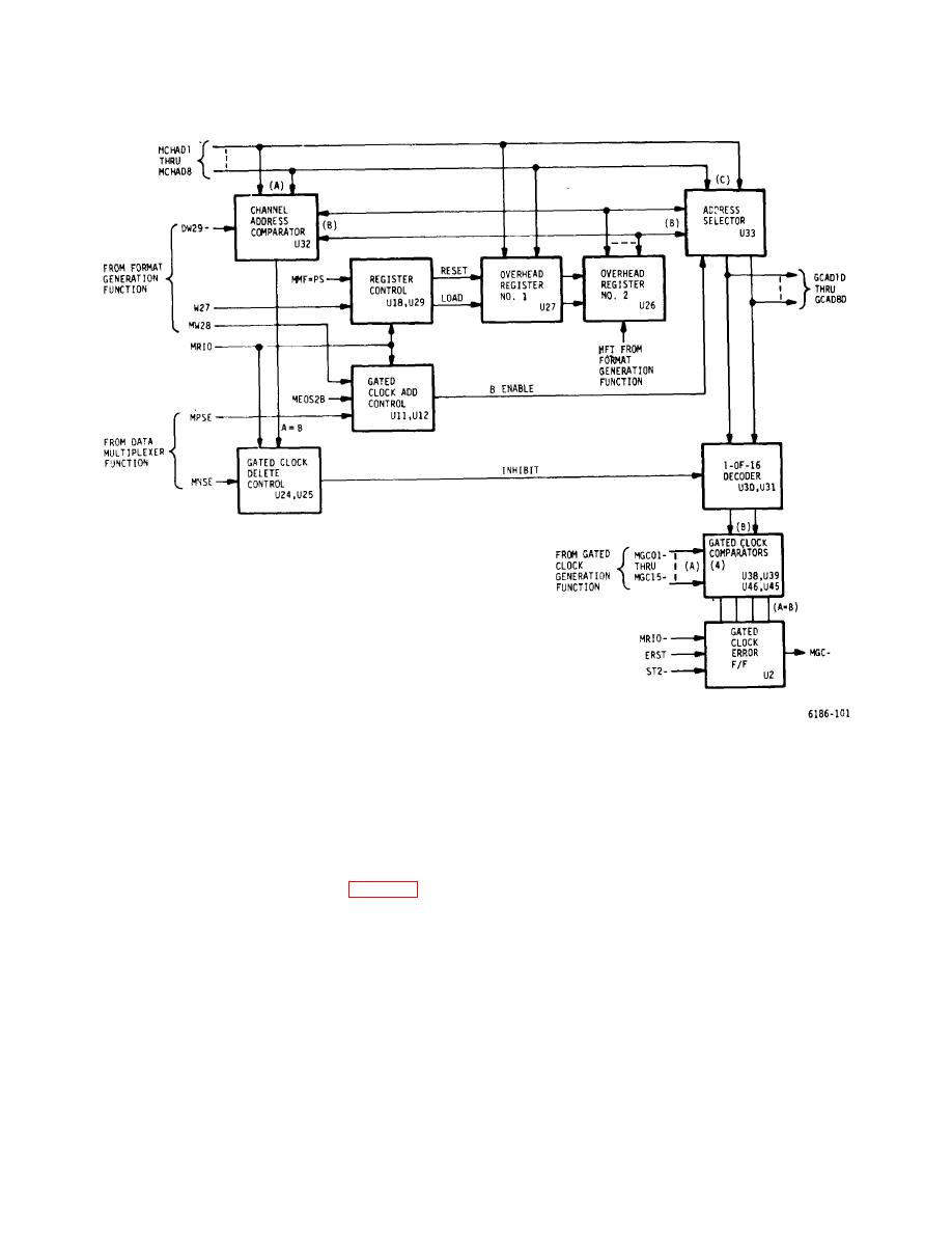
Figure 5-26. GC/DM Card, Gated Clock Generation Diagnostic Circuits - Block Diagram |
|
||
| ||||||||||
|
|
 T.O. 31W2-2GSC24-2
TM 11-5805-688-14-1
NAVELEX 0967-LP-545-3010
Figure 5-26. GC/DM Card, Gated Clock Generation Diagnostic Circuits - Block Diagram
The codes also contain the synchronization codes that
level signal, through inverter U13-4 during word 27, to J-
are used in the frame sync card to detect frame
K flip-flop U3-5, AND gate U19-3; and AND gate U19-6.
synchronization of the incoming serial data stream. The
The words 28/29 decoder is a two-bit shift register
ROM generates one bit from each output during each
consisting of J-K flip-flops U3-5 and U3-9. when word 27
word. The addresses from the word counter apply
is applied to U3-5, it is clocked through the two stages by
sequential addresses in the other shown in table 5-5.
end-of-scan signal MEOS2B to generate words 28 and
29. Word 29 signal MW29 is applied to word 29 activity
5.-334. The word 27 decoder, consisting of AND gates
detector Ul-10 in the composite error detector circuits for
U15 and U4 and inverters u13 and U21, applies a high
diagnostic purposes.
5-88
|
|
Privacy Statement - Press Release - Copyright Information. - Contact Us |
