 |
|||
|
|
|||
|
Page Title:
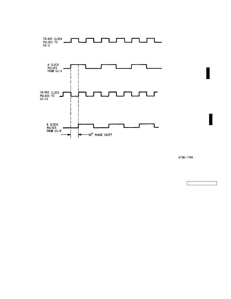
Figure 5-49. A Clock and B Clock Waveform Diagram |
|
||
| ||||||||||
|
|
 T.O. 31W2-2GSC24-2
TM 11-5805-688-14-1
NAVELEX 0967-LP-545-3010
Figure 5-49. A Clock and B Clock Waveform Diagram
At the same time, the dc ramp voltage is applied to the
5-640. The functional operation of the four +5-volt
non- inverting input of AR7-5. Since the threshold
regulators on the +5-volt regulator card A2 are basically
voltage has increased, a more positive (longer time
the same as the operation described in paragraph 5-639.
duration) dc ramp voltage level is required to cause the
As shown on the +5-volt regulator card schematic, one
output voltage from AR7-10 to go more positive to cutoff
voltage comparator circuit and error amplifier serve the
switch Q8. The longer it takes to cutoff Q8, the longer
four +5-volt regulator circuits. Any change in the +5-volt
that one-shot multivibrator U3 is allowed to conduct when
regulated out- put is sensed by voltage comparator AR4-
it is triggered on by a B clock pulse. In turn, the more
12. The comparator, in turn, produces a voltage change
negative that the regulated -12 volts be- comes, a less
to the input of AR4-10. The output from AR4-10 is
positive voltage level is established for the threshold
applied as the threshold voltage to the inverting inputs of
voltage applied to AR6-7. This lower threshold voltage
the high-speed comparators in the four +5-volt power
level results in a narrower pulse being produced from
regulator circuits. The four drive pulses from the four
U3.
regulators are produced through pulse transformers T2,
T4, T6, and T8.
Change 2 5-175
|
|
Privacy Statement - Press Release - Copyright Information. - Contact Us |