 |
|||
|
|
|||
|
Page Title:
DETAILED CIRCUIT DISCUSSION-CONT. |
|
||
| ||||||||||
|
|
 T.O. 31W2-2GSC24-2
TM 11-5805-688-14-1
NAVELEX 0967-LP-545-3011
This condition presents the SD3 and SD2 data bits as
logic) to the five data selectors are paralleled. The select
outputs B1 through B10 that are applied in parallel to the
input signal combinations to select the pairs of SD2,
three stuff command code comparators. In a given word
SD3, or odd-bit data are listed below. The data se-
time, the number of sequential bits applied as a B output
lectors are sampled at the RIO rate and are sequenced
is equal to n+l between 16 and 32 bits.
so that B1 through B10 provide a parallel set of data bits
contained in 10 consecutive words.
For example,
5-520. When signal DPUBO is a zero, rep- resenting an
assuming that B1 represents bit 3 in a given word,
even number of ports in use, the LSB preset input to 4-
signals B1 through B10 represent the third data bit in 10
bit address counter U57 from inverter U36-4 is a count of
consecutive words being monitored. Time- wise, signal
one. Also, the preset signal applied to flip-flop U64-5 is
B10 represents the first word applied to the VLSR and is
effectively removed by the high-level signal from U36-4.
the first word being monitored; B1 is the last word
This configuration enables the odd data bit functional
applied to the VLSR in the 10-word sequence and is the
circuits in the VLSR. In this configuration, the primary
10th word of the group being monitored. Note that odd-
shift register continues to operate as described
numbered signals (B1, B3, B5, B7, and B9) are barred
previously, but the initial write/read sequence is delayed
signals and even-numbered signals (B2, B4, etc) are
one RIO time for the processing of the odd data bit as
unbarred. This condition is caused by inversion of the
described in the following paragraph.
SD2 and SD3 signals in the R.A.M. outputs. In the
loopback action involved, the even-numbered data bits
5-521.
When a compare is made in ad- dress
are subject to double inversion to produce unbarred
comparator U65, the A=B signal presets 4-bit address
output signals.
counter U57 to a count of one and also applies an enable
signal to one input of AND gate U55-8. This occurs when
signal RIO- is present. At the next RIO time, both inputs
to AND gate U55-8 are high and flip-flop U64-5 output is
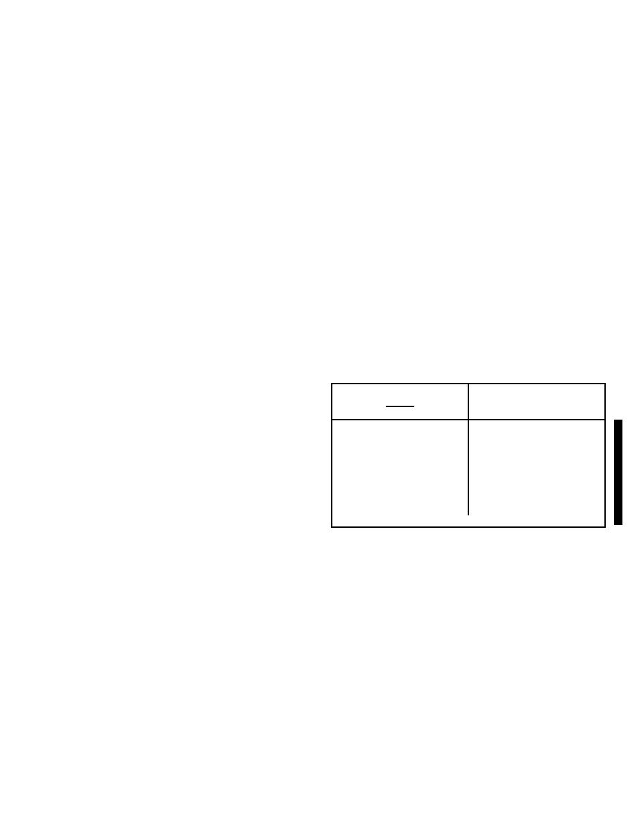
Select
Active Data
low and its -6 output is high. This inhibits half-rate flip-
Inputs
Selector
flop U56-5 from generating a write en- able signal,
A1
A0
Input and Output
during the next RIO- time, to the R.A.M.'s. In turn, the
high U64-6 output allows the following RIO signal to set
L
L
A1 & A2
odd-bit address flip-flop U64-9 so that the next RIO-
signal clocks the SD3- data into odd-bit shift register
L
H
B1 & B2
U39. At the same time, the data bits in shift registers
U39, U15, and U7 are shifted one position, and the A
H
L
(not used)
input to each data selector is high to enable the 1C3 and
2C3 data paths in each of the five data selectors. The
H
H
C1 & C2
action enables the odd-bit data in the 10 words (B1
through B10) to be applied through the data selectors
(U48, U31, U23, U16, and U8) to the three stuff
command code comparators (U6, U14, U22, U30,
5-523. Since the operation of the three code comparator
U38, and U46).
circuits is identical, only the operation of positive stuff
code comparator U6, U14 is described.
5-522. The A and B select inputs (labeled A0 and A1 on
Change 1 5-138
|
|
Privacy Statement - Press Release - Copyright Information. - Contact Us |
