 |
|||
|
|
|||
|
Page Title:
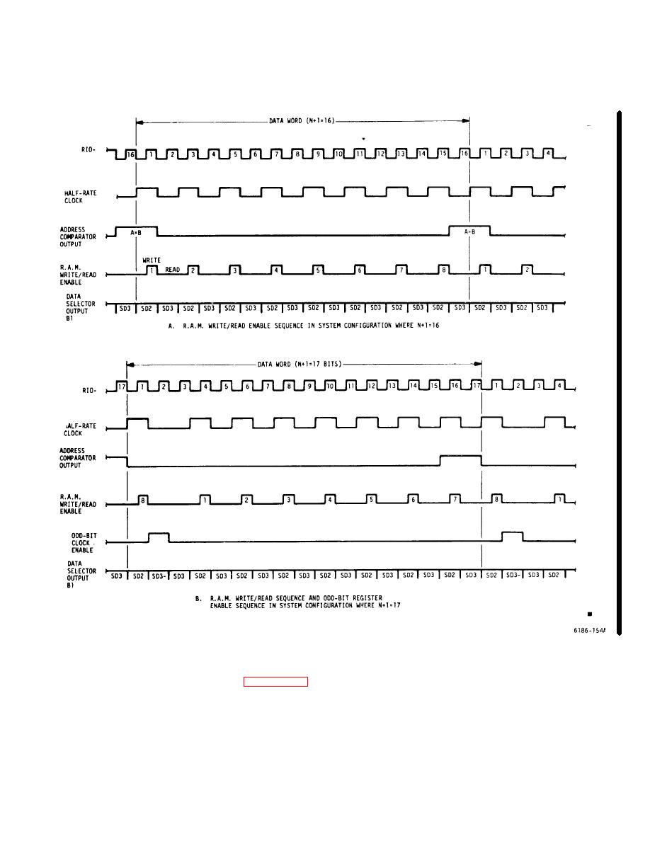
Figure 5-38. FS Card, Data Selector Outputs - Waveform Diagram |
|
||
| ||||||||||
|
|
 T.O. 31W2-2GSC24-2
TM 11-5805-688-14-1
NAVELEX 0967-LP-545-3011
Figure 5-38. FS Card, Data Selector Outputs - Waveform Diagram
words with an even number of bits are described first.
5-498. VLSR Block Diagram Discussion (Figure FO-
After this discussion, the circuits configured to process
8). In the following block diagram discussion of the
the data words with an odd number of data bits are
VLSR,
the circuits configured to process data
described to show the insertion of the odd bit of data in
the parallel readout of bits 1 through 10 from the VLSR.
Change 1 5-131
|
|
Privacy Statement - Press Release - Copyright Information. - Contact Us |