 |
|||
|
|
|||
|
Page Title:
DETAILED FUNCTIONAL CIRCUIT DISCUSSION-CONT. |
|
||
| ||||||||||
|
|
 T.O. 31W2-2GSC24-2
TM 11-5805-688-14-1
NAVELEX 0967-LP-545-3010
The output from multiplexer U6 is applied through AND
address signals from U7 are also applied to AND gates
gate U30-11 and inverter U45-8 to produce units address
U32-6, U22-6, and U11-12, together with inverter U14-10
signal UA0 that is applied to the front panel. The other
in the lamp display decoder logic circuits. In normal
digits that form the card address applied to the front
operation, the inputs to the four exclusive OR gates
panel are units address signals UA1, UA2, and UA3, and
(U28) from inverter U27-8 are low and the outputs from
tens address signals TA0 and TA1 from converter U12.
inverter U27- 10 to five OR gates (U19, U11, and U20)
The card ad- dress produced at this time represents the
are high. Therefore, the 3-bit address 010 from U7
card location associated with the overhead address
inhibits AND gate U32-6 and enables AND gate U19-3.
count (MOHO through MOH3) applied to counter U8.
The low output from U19-3 is applied to OR gate U19-11,
The binary coded decimal (BCD) outputs from the
which, in turn, generates card fail signal FAIL that is
combination of inverter U45-8 and binary-to-BCD
applied to the Seq card to indicate a card failure for the
converter U12 are listed below. The number equivalent
remote alarms. A FAIL signal is not decoded for an
for each output is the number that is displayed on the
OOTXX, DLOT-, or MLOT- signal. The output from AND
front panel. Numbers not shown are created by the sum
gate U19-3 is also processed through OR gate U19-8
of the numbers listed below. For example, the number 9
and exclusive OR gate U46-3 to generate multiplexer
requires signals UA0 and UA3. The number 19 requires
card error signal LMCRD, which lights the
signals UA0, UA3, and TA0.
MULTIPLEXER CARD indicator on the front panel. The
GS (pin 14) output from U7 is also applied to the decoder
logic circuits as part of the decoder logic function. The
output from U7-14 is low for each error signal applied to
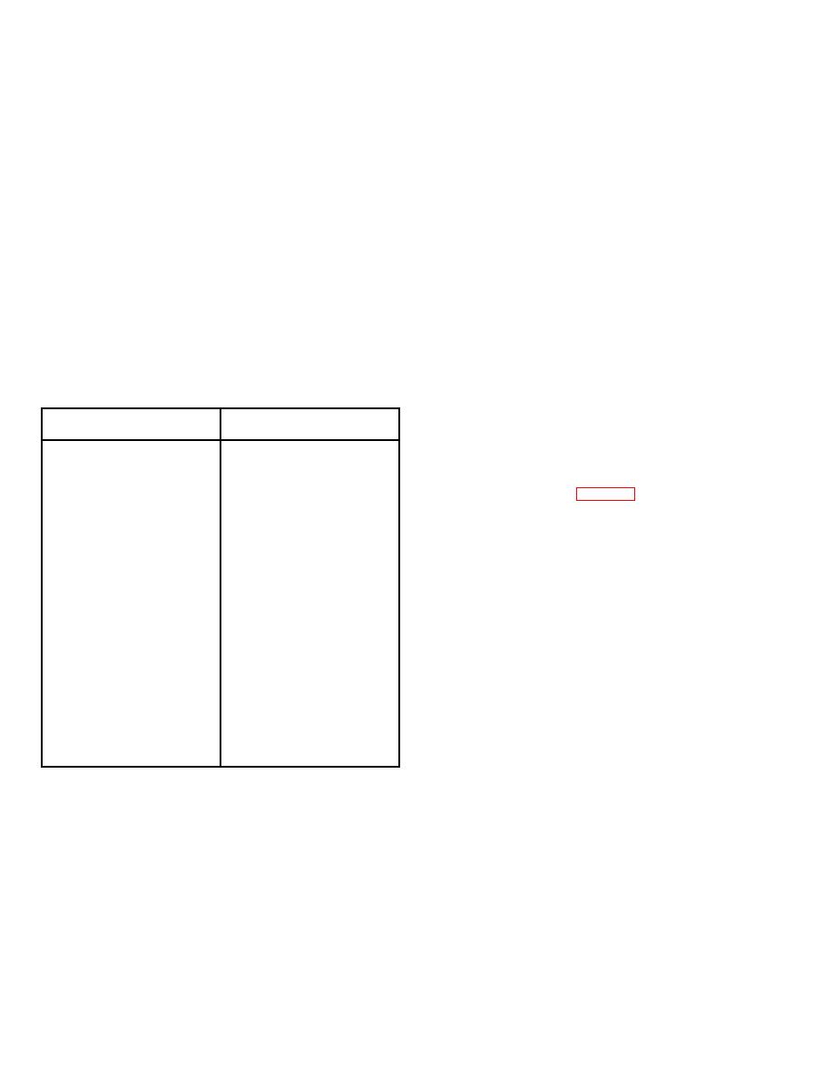
Number Shown on
U7, except loss of timing signal MLOT-; for this one
Output Code
Front Panel
signal, the output from U7-14 is high. The GS output
UA0
1
and the 3-bit address select signals from U7 to the
decoder logic for each of the possible nine error input
UA1
2
conditions are listed in table 5-7.
UA0 + U A1
3
5-595. Demultiplexer positive stuff signal DPSA- is
processed through flip- flop U17-10, and the associated
UA2
4
Units
channel overhead address count signals (DOHO through
DOH3) are processed through counter U9 in the same
UA0 + UA2
5
basic sequence described previously for multiplexer
signal MPSA- and the channel overhead address count
UA1 + UA2
6
signals (MOH0 through MOH3).
UA0 + UA1 + UA2
7
5-596. Multiplexer common card error priority encoder
U33 monitors diagnostic error signals MLEOS-, MDM-,
UA3
8
MSEQ-, MGC-, and MTMOG- from the multiplexer
common cards. When a low-level error signal is applied
UA0 + UA3
9
through its associated exclusive OR gate, a low-level
signal is applied to an input on U33. Outputs Y0 and Y2
TA0
1
from U33 contain the card address code associated with
Tens
the specific error in- put. The Y0 and Y2 outputs are
TA1
2
applied to the I1 inputs of multiplexers U6, U5, and U4 in
the card address encoder.
5-594. One or more digits of the 010 3-bit select
5-161
|
|
Privacy Statement - Press Release - Copyright Information. - Contact Us |
