 |
|||
|
|
|||
|
Page Title:
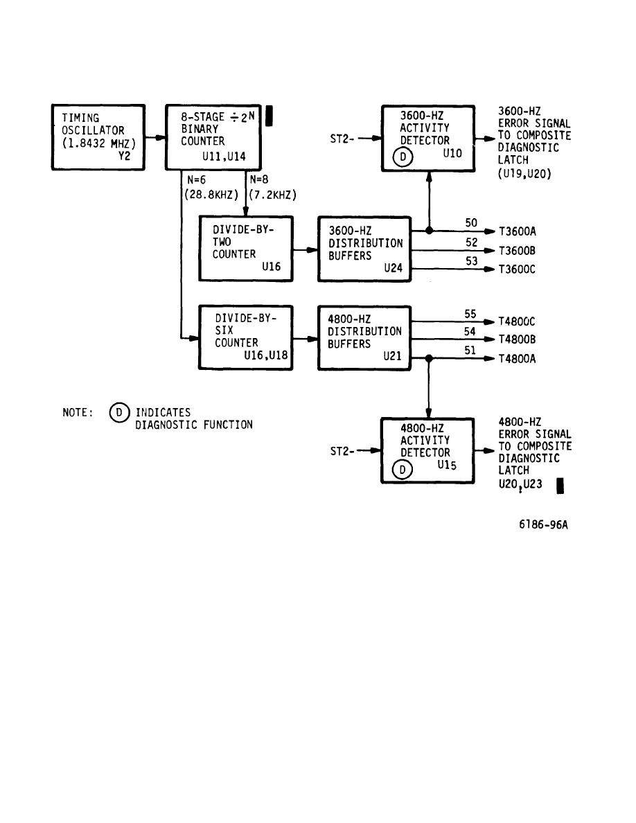
Figure 5-29. RT Card, Transition Encoder Timing Circuits - Block Diagram |
|
||
| ||||||||||
|
|
 T.O. 31W2-2GSC24-2
TM 11-5805-688-14-1
NAVELEX 0967-LP-545-3010
Figure 5-29. RT Card, Transition Encoder Timing Circuits - Block Diagram
The N=6 (28.8 kHz) output from the eight-stage N
the composite OR gate and latch circuits on the card
when timing signals T3600A and T4800A are missing.
binary counter is applied to the divide-by six counter,
The two activity detector circuits are set and held in the
which, in turn, supplies the 4800-Hz timing signals to the
error state by self-test signal ST2 when the SELF TEST
4800-Hz distribution buffers. The distribution buffers
switch on the front panel is set to the on (up) position.
produce 4800-Hz timing signals T4800A, T4800B, and
When the SELF TEST switch is set to the off (down)
T4800C that are routed to the channel card locations.
position, signal ST2 is removed and the activity detector
The 3600-Hz and 4800Hz activity detectors sample the
circuits return to their no-error state.
timing signals and generate diagnostic error signals to
Change
5-100
|
|
Privacy Statement - Press Release - Copyright Information. - Contact Us |
