 |
|||
|
|
|||
|
Page Title:
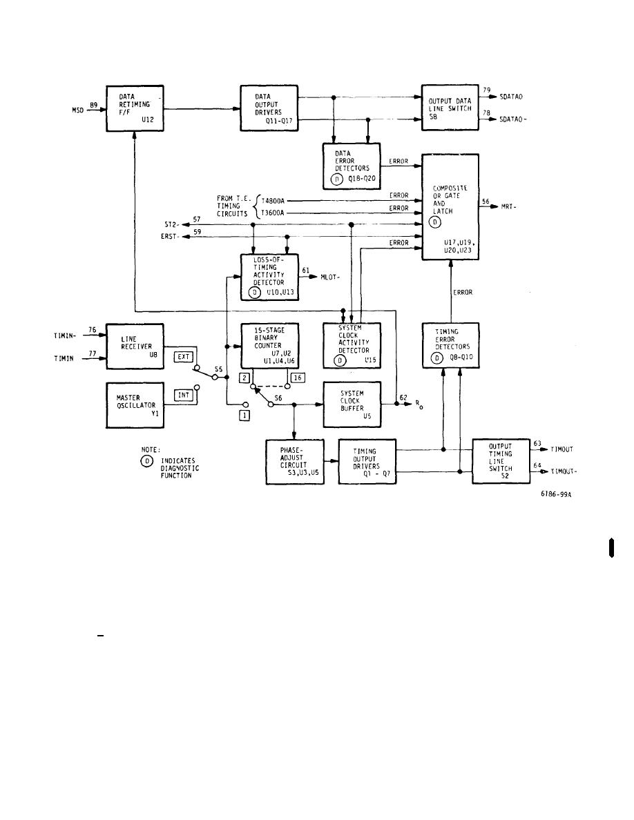
Figure 5-28. RT Card, Data and Timing Circuits - Block Diagram |
|
||
| ||||||||||
|
|
 T.O. 31W2-2GSC24-2
TM 11-5805-688-14-1
NAVELEX 0967-LP-545-3010
Figure 5-28. RT Card, Data and Timing Circuits - Block Diagram
n
to an eight-stage 2 binary counter. The N=8 (7.2 kHz)
Setting the SELF TEST switch to the off (down) position
applies reset signal ERST to the circuits and forces them
output from the counter is applied to the divide-by-two
to their no-error state.
counter, which, in turn, supplies the 3600-Hz timing
signals to the 3600-Hz distribution buffers.
The
5-378. The transition encoder timing circuits (figure 5-
distribution buffers produce 3600-Hz timing signals
29) generate timing signals T3600 (3600 Hz) and T4800
T3600A, T3600B, and T3600C that are routed to the
(4800 Hz) that are used by the TE/TR channel cards in
channel card locations.
the multiplexer.
The timing oscillator generates a
1.8432MHz (+0.01 percent) timing signal that is applied
Change 1 5-99
|
|
Privacy Statement - Press Release - Copyright Information. - Contact Us |
