 |
|||
|
|
|||
|
Page Title:
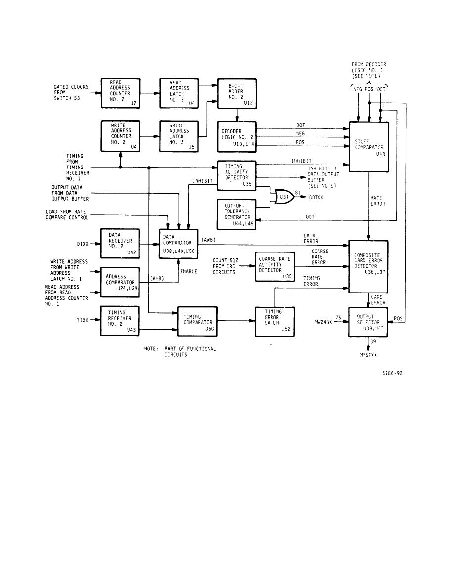
Figure 5-14. RCB Card, Diagnostic Circuits - Block Diagram |
|
||
| ||||||||||
|
|
 T.O. 31W-2GSC24-2
TM 11-5805-688-14-1
NAVELEX 0967-LP-545-3011
Figure 5-14. RCB Card, Diagnostic Circuits - Block Diagram
5-185. When the rate compare control circuits generate
is the same as the write address stored in the
a load signal, the data bit (DIXX) from data receiver No.
comparator, an enable signal (A=B) is applied to the data
2 is loaded in the data comparator, and the write address
comparator to enable the data compare function. The
from the write address latch associated with the data bit
data bit stored in the data comparator is compared with
is loaded into the address comparator. The address
the data bit in the data output buffer at this time. Since
comparator samples the read address out of the read
the read and write addresses are the same, the data bits
address counter. When the read address
being
compared
should
also
be
5-45
|
|
Privacy Statement - Press Release - Copyright Information. - Contact Us |
