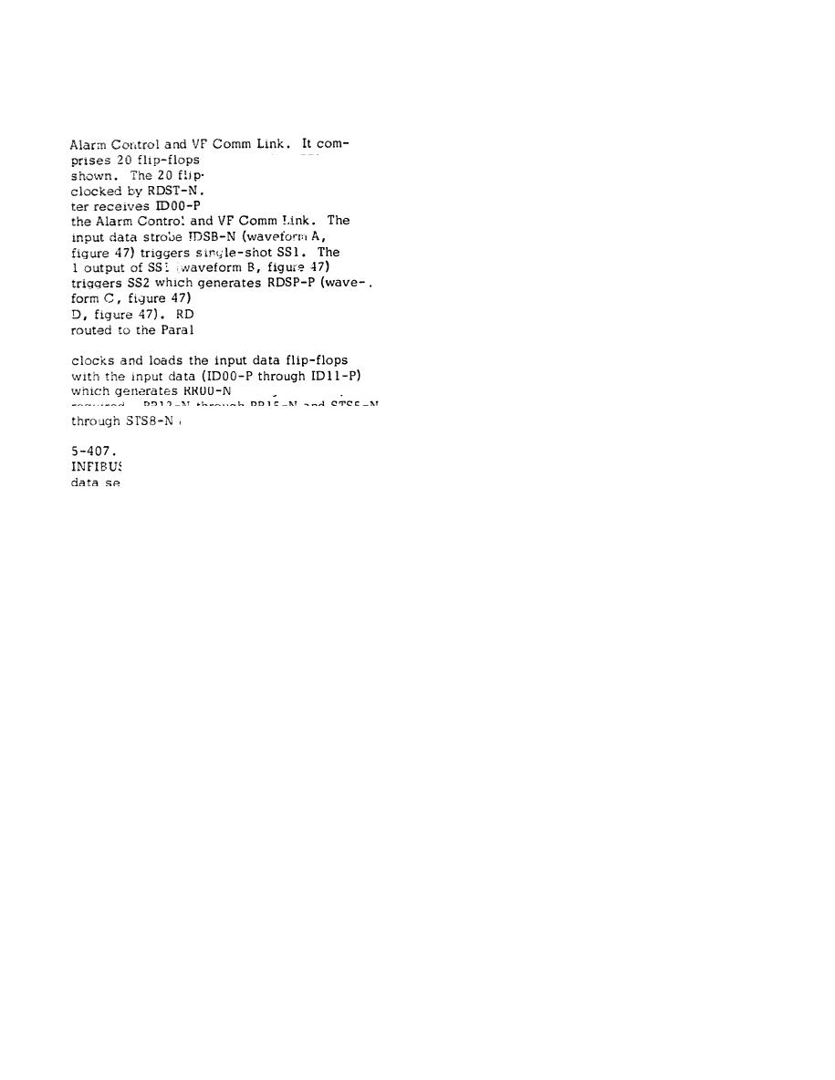
 |
|||
|
|
|||
|
Page Title:
PARALLEL I/O DATA OUTPUT AND CONTROL REGISTER CIRCUIT |
|
||
| ||||||||||
|
|
 T.O. 31S5-4-308-l
TM 11-5805-663-14-13
NAVELEX 0967-464-0010
through 4A inputs to the Yl through Y4,
output, respectively. This condition couples
with flip-flop FFl
the control register data to the Parallel I/O
-flops are simultaneously
data output and control register circuit.
The input data regis-
though ID11-P from
5-410. When the Parallel I/O is slaved
to read status data, the Parallel I/O address
receivers and recognition circuit generates
MPXA-P (MPXB-P and BOLA-P low). Ml
through M4 couples the 1C1 and 2Cl inputs
to the Yl and Y2 outputs, respectively. MS
and RDST-N (waveform
couples the 1A through 4A inputs to the Yl
SP-P and RDST-N are
through Y4 outputs, respectively. M6
lel I/O read/write
couples the 1B through 4B inputs to the Yl
control status circuit. RDST-N also
through Y4 outputs, respectively. This
condition couples the Parallel I/O and
through RR15-N, as
Alarm Control and VF Comm Link function
status data to the Parallel I/O data output
are always genera ted.
and control register circuit..
All data to be placed on the
5-411. When the device number is to be
S data lines is `first selected by the
placed on the INFIBUS data lines during
lectors M1 through M6. Ml through
an interrupt request, the Parallel I/O address
M4 are dual four-line to one-line selec-
receivers anti recognition circuit generates
tors whose output data is determined by
MPXA-P and MPXB-P, and the Parallel I/O
the value of MPXA-P and MPXB-P. MS and
INFIBUS access circuit generates BOLA-P.
M6 are each quad two-line to one-line
Ml through M4 couple the lC3 and 2C3 inputs
s e l e c t o r s . The output data of M6 is deter-
to the Yl and Y2 outputs, respectively.
mined by the value of MPXA-P.
MS couples the 1B through 4B inputs to
The output data of MS is determined by the
the Yl through Y4 outputs, respectively.
value of BOLA-P.
This condition couples the device number,
DN04-N through DN11-N and STS5 through
5-408. When the Parallel I/O is slaved to
STS8, to the Parallel I/O data output
read the data from the Alarm Control and
a n d control register circuit.
VF Comm Link function, MPXA-P, MPXB-P
and BOLA-P are low. Ml through M4 couple
the lC0 and 2C0 inputs to the Yl and Y2
PARALLEL I/O DATA OUTPUT AND
o u t p u t s , respectively. M5 and M6 couple
CONTROL REGISTER CIRCUIT.
the 1A through 4A inputs to the Yl through
Y4 outputs, respectively. This condition
5 - 4 1 3 . G e n e r a l . The Parallel I/O data
couples the data from input data register,
output and control register circuit stores
RROO-N through RR15-N, to the data out-
data that is to be transferred to the Alarm
put and control register circuit (DOOA-N
Control and VF Comm Link Function. Also,
through D15A-N).
the Parallel I/O data output and control
register circuit stores control words which
5-409. When the Parallel I/O is slaved
controls read or write operations that are
to read the Parallel I/O control register
to be done with the Alarm Control and VF
data from the Parallel I/O data output and
Comm Link Function.
control register circuit, the Parallel I/Q
address receivers and recognition circuit
5 - 4 1 4 . Detail Analysis (see figure 48).
generates MPXB-P (MPXA-P and BOLA-P
When master reset, MRES-N, is generated
low). M1 through M4 couple the lC2 and
on the INFIBUS I10 inverts MRES-N
2C2 inputs to the Yl and Y2 outputs, re-
and the output of I10 activates gate G8
spectively. M5 and M6 couple the 1A
which generates GRSA-N. GRSA-N is in-
|
|
Privacy Statement - Press Release - Copyright Information. - Contact Us |
